

Hi All. I would like to create this post with all step by step guide with all info for PCB from Schematic to Fabrication and Assembly. This is a set action that I did a couple of times every time it seems that I can forget something, so this should use even as a guide for me for future PCB projects and fabrications.
In the intro let’s just add some definitions and explanations on what should happen in this process.
Also for this example, I will be using KiCad as a PCB design tool and I will fabricate and assemble PCB using JLCPCB.
There are a lot of alternatives for PCB design tools (Altium, EasyEDA, CircuitMaker …) and fabricators (PCBWAY, NEXTPCB…) but the process of generating should be more or less the same.
Check out my other related post
- https://blnlabs.com/how-to-add-usb-type-c-to-esp32-development-board/
- https://blnlabs.com/how-to-add-esp32-to-kicad/
Also check out my YouTube Video on the same topic
Prerequisites
Add Symbol Info
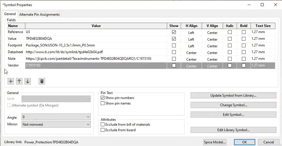
Of course, we need to have finished the design of the PCB and schematics at this stage in order to start with the steps to go from PCB to fabrication and assembly. Also, I would help a lot if you had planned at the start to fabricate your PCB design with JLCPCB or someone else because I added component info at the time when I created the schematic. If you have all the information fields when generating the BOM (Bill of materials), you will not need to edit almost anything in the final product. So, I add two fields in Symbol properties and those are:
- Note – Placing the link of the selected component to the JLCPCB component library
- Vendor – Add the component ID (JLCPCB Part number) for the selected component from JLCPCB
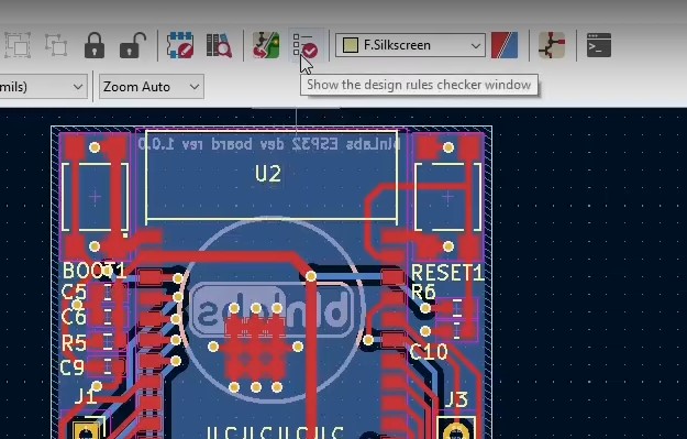
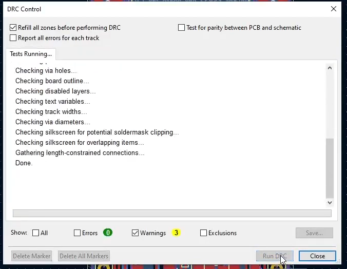
Check DRC
Next, after I finished with the PCB design I ran a DRC check.
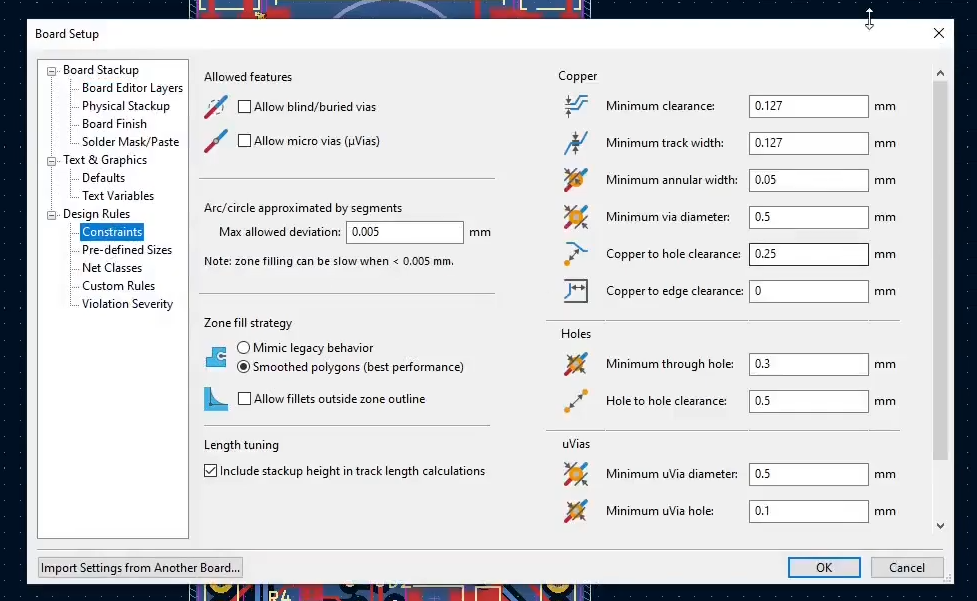
A quick look inside Design Rules
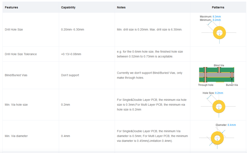
There is maybe an opportunity for another post where I will explain how I configured my design rules that are in compliance with the fabricator, in this case, JLCPCB, but the good way is to open Board Setup shown in the image below and try to map all values from JLCPCB Capabilities to your Board Setup.
But as I said this exceeds the topic for this post, and I will now return to Fabrication and Assembly steps.
Fabrication
Fabrication is the process that requires the next inputs, and the output is a finished PCB board without any components.
- Gerber files
- drill files
- Some settings on the JLCPCB site
Gerber
The first step in the fabrication process of PCBs, so just short. What are Gerber files and why do we need them?
The Gerber format is an open, ASCII, vector format for printed circuit board (PCB) designs.[1] It is the de facto standard used by PCB industry software to describe the printed circuit board images: copper layers, solder mask, legend, drill data, etc.
by Wiki
Understand layers
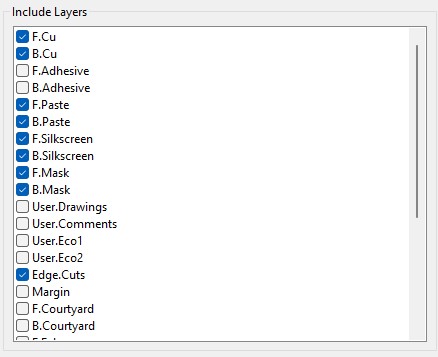
We are exporting the data about copper traces, solder masks, and everything that is needed by fabricator JLCPCB. Here we need to know the list of layers that we need, and that can be different depending on your project. If we are creating a single layer, the board we need only copper, silk screen, and solder mask for the top or bottom, and if we want to create a 2 layer board that list will be doubled. Same as in 4 layer board. So, we need to know what each layer stands for and select that layer from the export.
And let us go over step by step:
- F.Cu – Front Copper (Top Layer) Layer of copper used for signals and power in two-layer design
- B.Cu – Back Copper (Bottom Layer) Layer of copper used mostly for ground plain in two-layer design
- F.Paste and B.Paste – Front and Back Paste layers are generally called stencil. This will be the area in which soldering paste needs to be applied for SMD components.
- F.Mask and B.Mask – Front and Back Mask layers are areas in which the solder mask needed to be removed in order to create mounting points for SMD and/or TH components.
- Edge.Cuts – Cut out layer, Layer that indicates the edge of the board.
- F.Silkscreen and B.Silkscreen – Front and Back Silkscreen layers are writhing on the PCB, which is just for cosmetic purposes or ease of use, the board would be functional without this layer.
I needed only these default, already selected layers for my board. If you are creating only one layer board, you need to select only layers which are on your designed side of the board. And, if you are creating 4 layer board, you will need additional two copper layers, but on that topic more in the next posts.
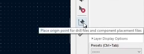
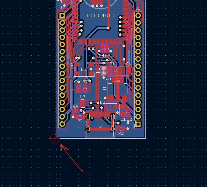
Add origin to PCB
Don’t forget to set your PCB origin. This should be most bottom left point of your board.
Export Gerber files
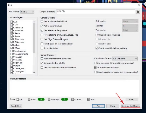
We are ready for Gerber export. Select File-> Fabrication Outputs -> Gerbers
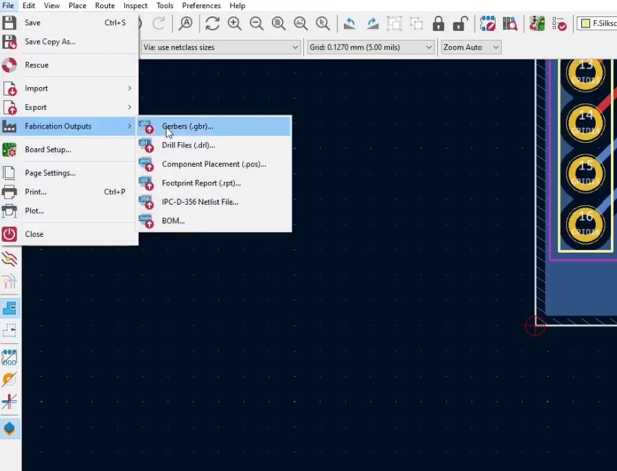
And default export options will be selected. This is fine, but we can now check whether our desired layers select or not, and check if the option Use drill/place file origin is also selected. This will use our previously set origin as the reference.
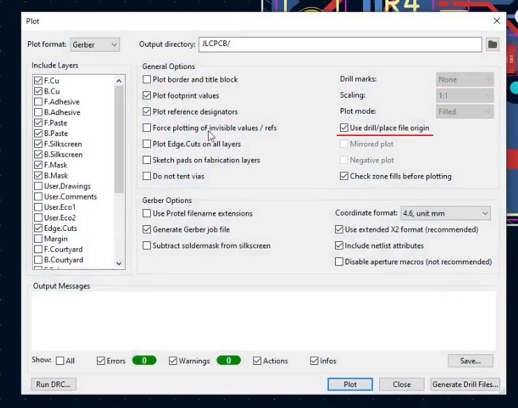
In this process, there will be a lot of generated files for maybe good practice is to create a separate folder for all fabrication data/files. Select the desired folder and click on Plot.
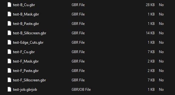
The output should look something like
Drill files
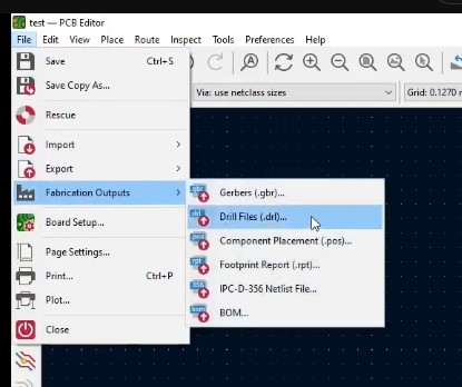
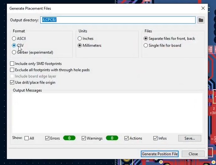
Also, for the final PCB, we need to have some holes. Holes for Trought-hole components, contactors … For this we need to generate drill files. That can be done from Gerber Plot Window, but by clicking Generate Drill Files…
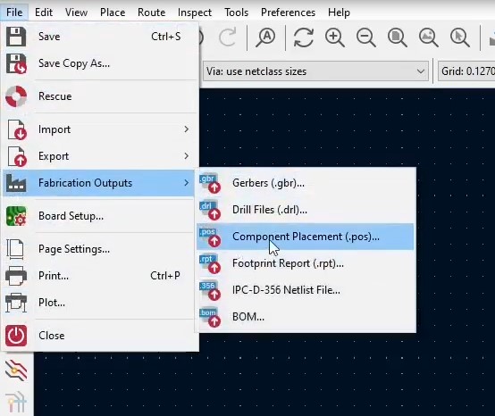
or by clicking on File->Fabrication Outputs -> Drill Files (.drl)
Next, select options Drill/place file origin, Millimeters for Drill Units shown in the image below.
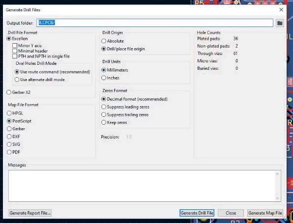
Click on Generate Drill Files and Generate Map File.
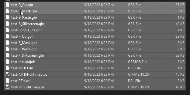
Now, I have everything that is needed for Fabrication with JLCPCB. Select all the files that are generated in this section and create a zip file.
Assembly
BOM – Bill of Materials
Definition of the BoM from Wiki
A bill of materials or product structure (sometimes bill of material, BOM or associated list) is a list of the raw materials, sub-assemblies, intermediate assemblies, sub-components, parts, and the quantities of each needed to manufacture an end product.
Wiki
We need to create a BOM for the step-by-step process where we are going from PCB to fabrication and assembly, but only if we want to assemble our board as well. This step and Pick and place are not required if you want to assemble your board by yourself and you want to receive only bare PCB from JLCPBC. We need to provide a list of components that will be added to our PCB board in the assembly process. And if we did the steps in the Prerequisites chapter correctly this step is pretty much automatic.
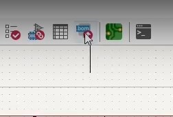
From the Schematic view that is the BOM icon. Click on it.
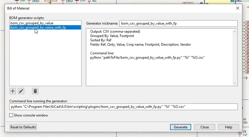
Next, select bom_csv_grouped_by_value_with_fp and click on generate.
The generated BOM should look something like
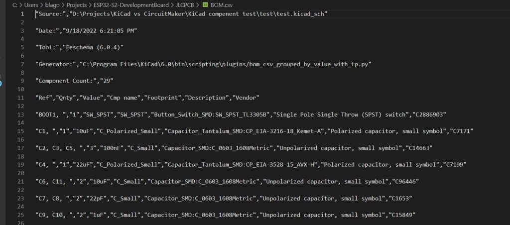
Here we can double-check if all components are assigned correctly and remove something if it is necessary. For this example I need to remove a couple of trought hole components from the BOM because JLCPCB doesn’t assemble TH components, so have this in mind when designing your board.

Pick and place
Surface-mount technology (SMT) component placement systems, commonly called pick-and-place machines or P&Ps, are robotic machines which are used to place surface-mount devices (SMDs) onto a printed circuit board (PCB). They are used for high speed, high precision placing of a broad range of electronic components, like capacitors, resistors, integrated circuits onto the PCBs which are in turn used in computers, consumer electronics as well as industrial, medical, automotive, military and telecommunications equipment. Similar equipment exists for through-hole components.
Wiki
This step is in the assembly process, with this we are given the instruction to Pick and Place the machine and which components should place in which section of the board.
In order for JLCPCB to understand this placement file we need to modify it a bit.
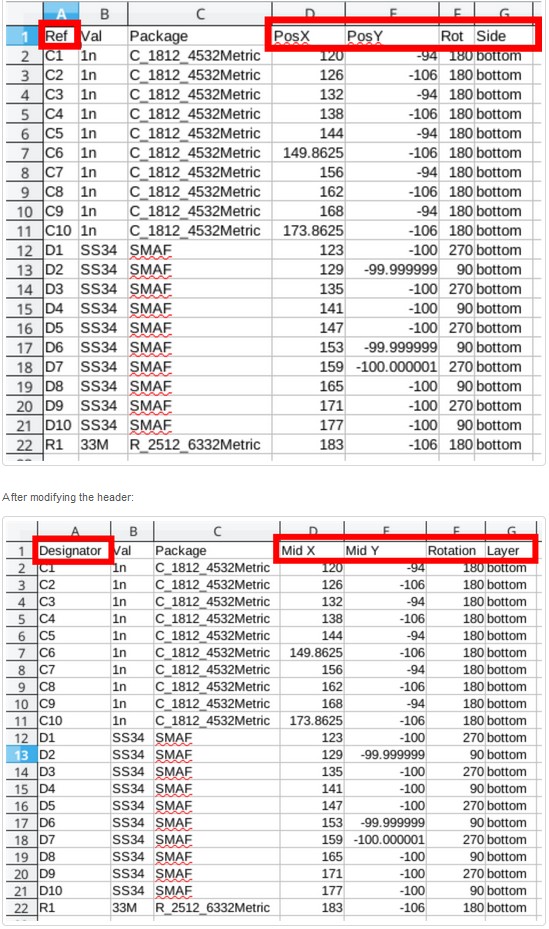
Simply I changed Ref
, PosX, PosY
, Rot
, and Side
to Designator, Mid X, Mid Y, Rotation, and Layer correspondingly. Info for this came from the official JLCPCB article How to generate the BOM and Centroid file from KiCAD. Cation! I didn’t use the BOM config from this article. I noticed that the default KiCad export worked fine.
JLCPCB settings
PCB Fabrication with JLCPCB
We are soon at the end. This should be the last step is this step-by-step where we go from PCB to fabrication and assembly. We have a couple of configurations for JLCPCB and that is shown in the images below.
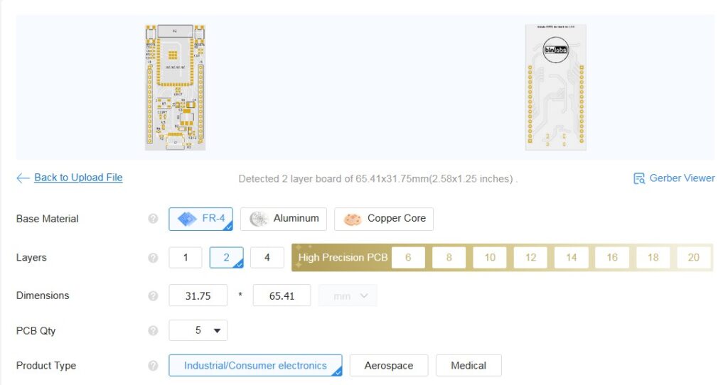
The image above is showing default configuration for PCB, which is FR-4 as the base material, Layers are set to 4, and so on …
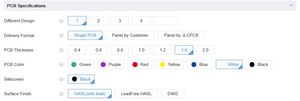
The second part is for copper trace width and via configuration. The default setting is fine here as well. One thing that I changed is Remove Order Number from No to Specify a location.
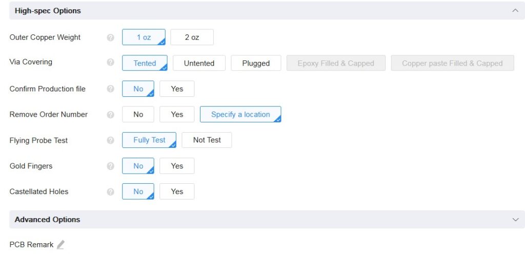
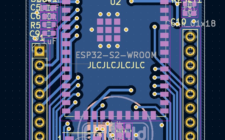
You just need to select that specific location with JLCJLCJLCJLC text In silkscreen.
PCB Assembly
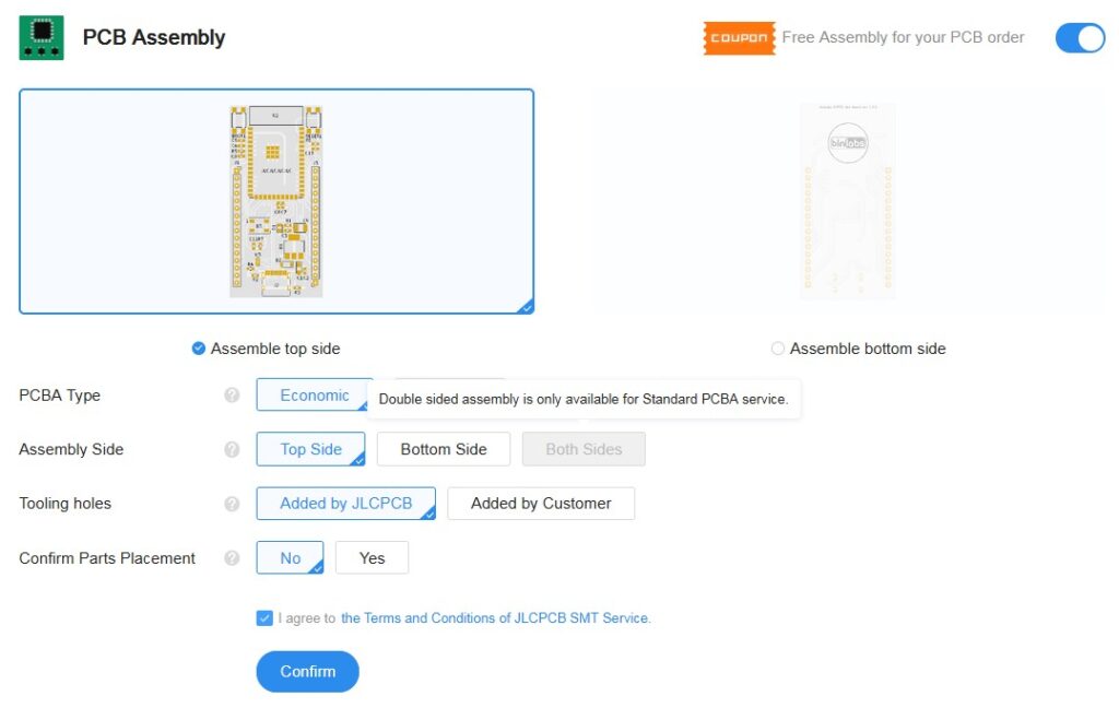
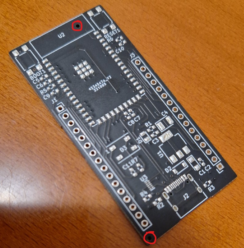
PCB Assembly has simple settings which maybe only a couple should be pointed out and those are the Assembly side (the selected side on which you have SMD components) and Tooling holes (Tooling holes are required when doing the assembly process. They can be added by you or JLCPCB). In this example, I left JLC PCB to add tooling holes, and in the image below we can see both of them.
Upload BOM and PicK&Place File
Next JLCPCB gives us the option to upload BOM and pick and place files, shown in the image below.
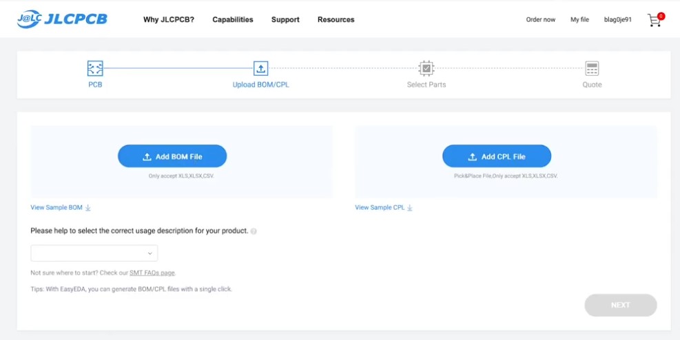
Just upload two files with a simple drag and drop to the correct place. Then JLCPCB offers us the possibility to check BOM and select parts for availability.
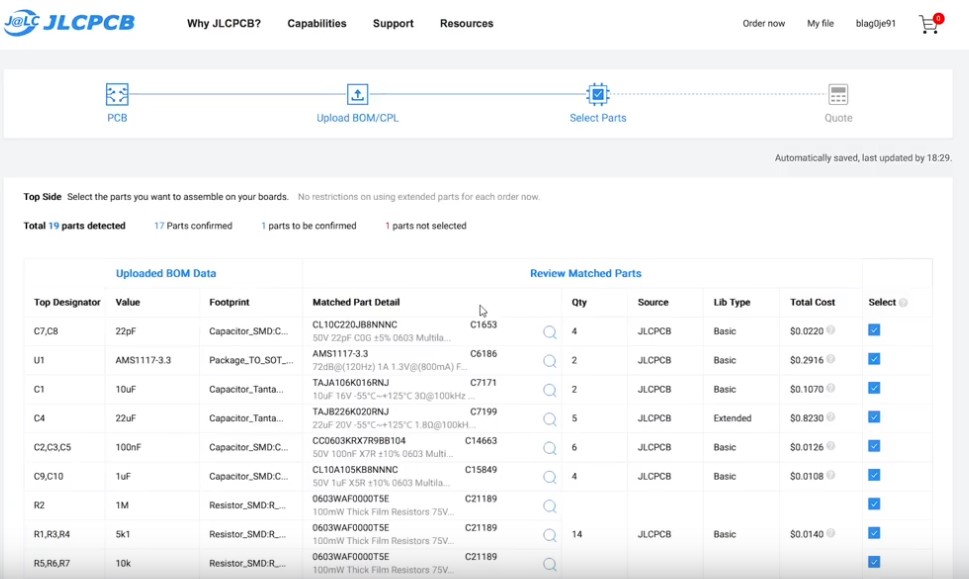
Then we are combining BOM import and pick and place file into one model in JLCPCB. This is final check befor fabrication and assembly. Here we need to be carefull. Here we need to check is pick and place file exported correctly, and updoped pick and place files if needed. I my case, I have couple of components missplaces and I needed to update pick and place file.
ESP32 was moved a bit to the top and it needed to be pushed down. On the other hand voltage regulator U1 is not correctly orientated.
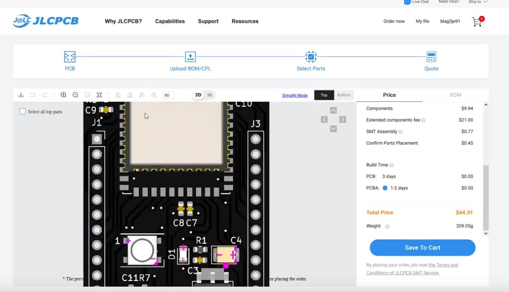
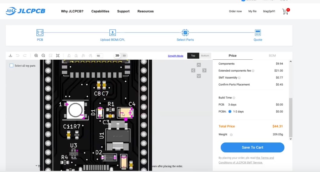
This can be easier done by changing a bit pick&place file that I detiled explained in YouTube view linked below.
Final Words
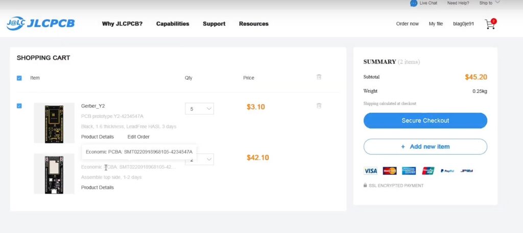
And that is it. In the image above I added the final step. You just need to press Checkout. This is meant to be step-by-step instructions on how to go from PCB to fabrication and assembly with JLCPCB and for PCB design I used KiCad. This is more a less general process, and it should be simular if you are using different PCB desing software and different PCB manifacture. You will always need to export Gerber, drill, BOM and pick and place files. So, this is it. Please comment down did you manage to create your own PCB, and did this process helped you in anyway? What did you make? Stay tuned for my next project and see you in the next one. Take care.
Hello
This is Liam from PCBWay.
Deeply impressed by your blog content which means a lot to electronic enthusiasts.
I’d like to sponsor your project by providing free PCB prototyping,
only hoping for a slight promotion or a review about quality or service in return.
Would you be interested in partnering up?