

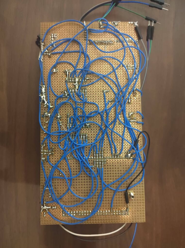
Hi All. I had a great Master thesis project a couple of years ago and I made a basic CNC plotter from old DVD/CD drives controlled by STM32. And that time, because of time constrain I didn’t make PCB for the motor driver circuit and because of that my custom board looked like this.

Now, I’m planning to continue work on the CNC plotter, but I can not work with this mess and I wanted to try to create PCB with jlcpcb. So, in this post, I will do PCB design in KiCad from scratch. In the end, PCB is looking like this:

Where to begin?
In order to design PCB, we need software for that purpose and that is KiCad. KiCad installation is pretty simple and I did it in the video below where I’m comparing the installation process of the Circuit Maker and KiCad.
And when we have KiCad installed we can continue creating schematic first.
Schematic
The first step in PCB design with KiCad is to create a schematic. This step can be a bit complicated if you need some custom components and for that components, you need to create symbols. But in this example we already have all components included in the default library, so we are fine.
Center peas of this board are of course STM32 blue pill development board and two l293d motor drivers. Because we need the only connector to plug in STM32 blue pill into our PCB we need a simple two-row connector. Also, there is the l293d symbol and footprint in the standard library. And that should look something like in the image below.

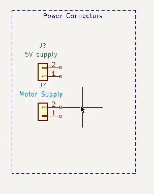
Next, we need to add Inputs (5V supply and motor supply) and Outputs Connectors (Connectors for Stepper motors, Servo motor and UART connector) and we will use the same connectors for the schematic.

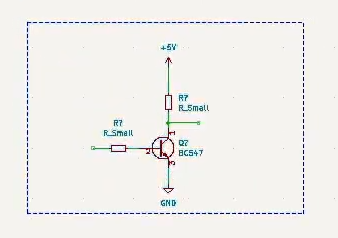
Lastly, we need to add one level shifter for 5V logic for the servo motor.
Connect Blocks
In order to finish the schematic we now need to link all blocks. The best way is to create global labels and to have the clean schematic. I covered every step in the creation of this schematic in the next YouTube video.
And at the end schematic should look something like this.

Final Words
Creating a schematic is the first step in creating a valid and working PCB. In a schematic, we need to check logic and connections and we need to make sure that everything is correct. Only after we have finished the schematic we can start with PCB design and trace routing. And, of course, I will create a post about that next time. Also, I have posted about starting STM32 development on Linux at the next link https://blnlabs.com/stm32-on-linux-in-2021/
At this point, I placed an order with jlcpcb and now I’m waiting for shipping, so I’m hoping that for a future post I will have some update about that as well. Until next that, stay safe and see you in the next one.